Description.

A simple telephone transmitter circuit that is ideal for transmitting the telephone conversation through small distances.The circuit is very simple and uses only few components.The entire circuit can be easily included in the telephone itself or in the junction box.The circuit is powered from the telephone line itself.

The transistor Q2 is wired as a a Colpitts oscillator to produce oscillations in the FM transmission band.The audio signal from the telephone line is coupled to the the base of Q2 to obtain the frequency modulation.The LED D1 acts as a power on indicator.

Circuit diagram with Parts list.

telephone_-bug-circuit.JPG

Notes.

  • Any radio frequency PNP transistor like A933 can be used for Q2.
  • For L1 make 8 turns of 0 .6mm dia enameled copper wire on a 3.6mm dia steel bolt.
  • For antenna use a 15cm long 0.6 mm dia copper wire.

Description.

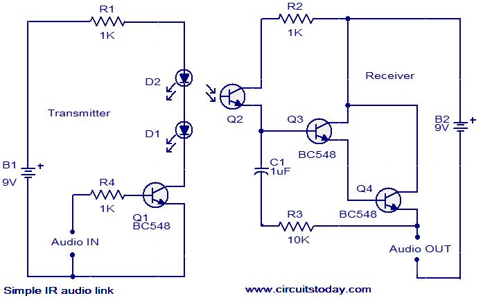
Here is a simple IR audio link that can be used to transmit audio signals up to 4 meters. The signal to be transmitted is applied to the base of Q1 via resistor R4.The transistor Q1 drives the IR transmitting diodes D1 and D2.The audio input will be modulated to the IR signals transmitted.
The transmitted IR signals will be picked by the photo transistor Q2.The emitter voltage of the transistor Q2 will change according to the sound modulated to the IR signal. The transistors Q3 and Q4 amplifies this signal to drive the speaker or headphone.C1 and R3 forms a filter to avoid interference from stray IR signals.

Circuit diagram with Parts list.

ir-audio-link-circuit

Notes

The circuit can be assembled on a general purpose PCB.

Use 9V PP3 batteries for powering the transmitter and receiver.

The phototransistor Q2 can be any NPN phototransistor like PNZ154, PNA1605F, BPW77NA or BPW85.

An 8 Ohm speaker or a headphone can be used to hear the sound.

Description.
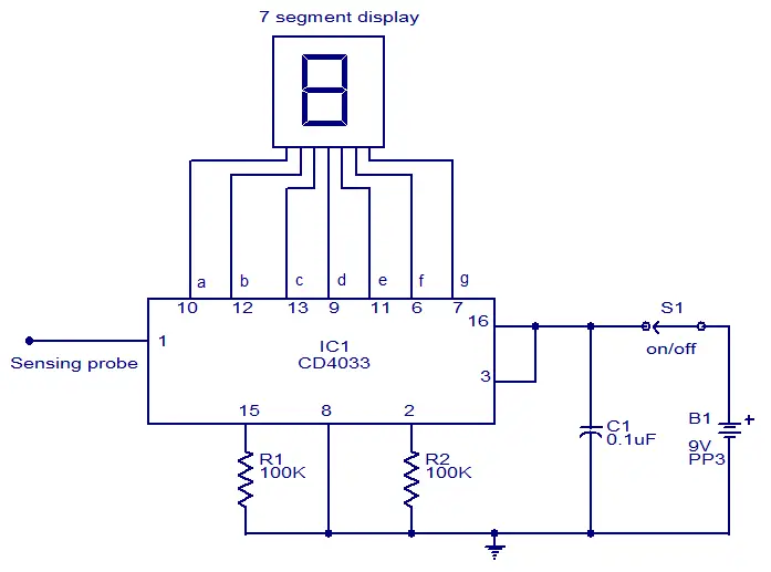
This circuit can be used to test whether mains voltage is present or not without having electric contact with mains line. The CMOS IC CD4033 is the heart of this circuit. The CD4033 consists of a 5 stage decade Johnson counter and an output decoder for converting the Johnson code to a 7 segment decoded output for driving 7 segment LED display. A 10cm long insulated copper wire connected to the clock pin (pin1) of the IC serves as the sensor. The sensor wire has to be placed in the vicinity of the mains wire to be tested. When there is no voltage in the mains line, no voltage will be induced in the sensor wire and the display will show a random digit. When there is voltage in the mains line, a small voltage will be induced in the sensor wire due to electromagnetic induction and this voltage is sufficient enough to clock the CMOS IC CD4033. Now the display will count from zero to nine and repeat.

Circuit diagram.

wireless mains indicator

Notes.

  • The circuit can be assembled on a Vero board.
  • Use 9V PP3 battery for powering the circuit.
  • Use a 10cm insulated wire as the sensor.
  • The IC must be mounted on a holder.
  • Switch S1 can be a miniature ON/OFF switch.

Made from the highest quality components, ValueRAM SO-DIMMs are designed to increase productivity and help your whitebook work faster. Backed by a lifetime warranty, free technical support and legendary reliability, Kingston ValueRAM is the standard in notebook memory upgrades.


How to Read Kingston ValueRAM Part Numbers


Notebook Top 5 Skus

KVR667D2S5/2G 2GB 667MHz DDR2 Non-ECC CL5 SODIMM
KVR667D2S5/1G 1GB 667MHz DDR2 Non-ECC CL5 SODIMM
KVR800D2S6K2/2G 2GB 800MHz DDR2 Non-ECC CL6 SODIMM
KVR533D2S4/1G 1GB 533MHz DDR2 Non-ECC CL4 SODIMM
KVR800D2S5/2G 2GB 800MHz DDR2 Non-ECC CL5 SODIMM

Performance and capacity redefined with Kingston's SD High-Capacity memory cards.

Kingston Technology's Secure Digital High-Capacity (SDHC) memory cards are fully compliant with the new Secure Digital Association 2.00 specification. They are a new performance class of SD memory cards designed to meet the storage demands of high-quality digital still and video cameras and other high-resolution image recording devices. Co-Logo Program

Storage Chart
To see how many images you can store on a Kingston SD card, click here. American Photo


Datasheet

Starting at 4GB, SDHC cards offer larger-volume data storage and optimized recording performance with support for FAT 32 file formats. In addition, Kingston’s SDHC cards use new speed "class" ratings known as Class 4 and 6 that deliver a minimum data transfer rate for optimum performance with SDHC devices.

Although identical in size to todays standard SD card, the new SDHC cards are designed differently and are only recognized by SDHC host devices. To ensure compatibility, look for the SDHC logo on cards and host devices (cameras, camcorders, etc.).

For added reliability and durability, our solid-state SDHC memory cards are built of nonvolatile memory components and have no moving parts that could wear out or break. All cards are 100-percent tested and are backed by a lifetime warranty and free live technical support.

This article has multiple issues. Please help improve the article or discuss these issues on the talk page.

* It needs to be updated. Tagged since September 2008.
* It is in need of attention from an expert on the subject. WikiProject Computing or the Computing Portal may be able to help recruit one. Tagged since November 2009.

PCI Express
Year created: 2004
Created by: Intel, Dell, IBM, HP
Supersedes: AGP, PCI, PCI-X
Width in bits: 1-32
Number of devices: Two devices, with one device each on each endpoint of the connection. PCI Express switches can be used to create multiple endpoints out of one endpoint to allow sharing of one endpoint with multiple devices.
Capacity Per lane:

* v1.x: 250 MB/s
* v2.0: 500 MB/s
* v3.0: 1 GB/s

16 lane slot:

* v1.x: 4 GB/s
* v2.0: 8 GB/s
* v3.0: 16 GB/s

Style: Serial
Hotplugging? Yes, if ExpressCard or PCI Express ExpressModule
External? Yes, with PCI Express External Cabling

PCI Express (Peripheral Component Interconnect Express), officially abbreviated as PCIe (or PCI-E, as it is commonly called), is a computer expansion card standard designed to replace the older PCI, PCI-X, and AGP standards. PCIe 2.1 is the latest standard for expansion cards that is available on mainstream personal computers.[1]

PCI Express is used in consumer, server, and industrial applications, as a motherboard-level interconnect (to link motherboard-mounted peripherals) and as an expansion card interface for add-in boards. A key difference between PCIe and earlier buses is a topology based on point-to-point serial links, rather than a shared parallel bus architecture.

The PCIe electrical interface is also used in a variety of other standards, most notably the ExpressCard laptop expansion card interface.

Conceptually, the PCIe bus can be thought of as a high-speed serial replacement of the older (parallel) PCI/PCI-X bus.[2] At the software level, PCIe preserves compatibility with PCI; a PCIe device can be configured and used in legacy applications and operating systems which have no direct knowledge of PCIe's newer features. In terms of bus protocol, PCIe communication is encapsulated in packets. The work of packetizing and depacketizing data and status-message traffic is handled by the transaction layer of the PCIe port (described later). Radical differences in electrical signaling and bus protocol require the use of a different mechanical form factor and expansion connectors (and thus, new motherboards and new adapter boards).
Description.
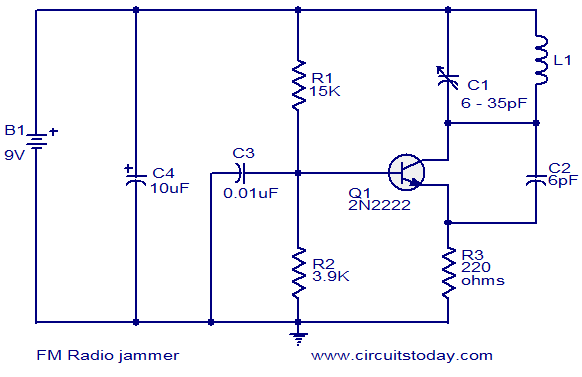
Circuit shown here can be used to jam FM radios in its vicinity. The circuit is nothing but a classic single transistor oscillator operating in the VHF region. Working principle of the circuit is very simple and straight forward. Powerful VHF oscillations from the circuit will interfere with the FM signals to nullify it. Jammer circuits like this are illegal in many countries and you must assemble this circuit on your own responsibility. This circuit is intended only for fun and i request you not to misuse it.
Circuit diagram.

FM radio jammer

Notes.

  • For L1 make 6 turns of 16AWG enamelled copper wire on a 9mm plastic former.
  • The circuit can be powered using a 9V PP3 battery.
  • For extended range, use an antenna.
  • A 30cm long wire connected anywhere on the coil will do for the antenna.
  • For better performance, assemble the circuit on a good PCB.

Description

A digital stop watch built around timer IC LM555 and 4-digit counter IC MM74C926 with multiplexed 7-segment LED display.MM74C926 consists of a 4-digit counter, an internal output latch, npn output sourcing drivers for common cathode,
7-segment display and an internal multiplexing circuitry with four multiplexing outputs.The counter advances on negative edge of the clock. The clock is generated by timer IC LM555.The circuit works off a 5V power supply. It can be easily assembled on a general-purpose PCB. Enclose the circuit in a metal box
with provisions for four 7-segment displays, rotary switch S1, start/stop switch S2 and reset switch S3
Testing

First, reset the circuit by pressing S3 so that the display shows ‘0000.’ Now open switch S2 for the stop watch to start counting the time. If you want to stop the clock, close S2. Rotary switch S1 is used to select the different time periods at the output of the astable multivibrator (IC1).

Circuit Diagram .Click to View in full size.

stopwatch-1.JPG

Description

This is a very useful circuit which when installed on your car gives the voltage of you car battery in a LED dot display form.The circuit is based on four comparators made of quad op amp LM324.The inverting inputs of IC are kept at at reference voltages 5.6V,5.2V,4.8V,4.4V respectively at pins 2,6,9,13 by resistors ,R3,R4,R5,R6.The battery voltage is directly fed to the nin inverting input throug the volatge divider arrangement using R1 and R7.When there is variation in the input supply the out put of each op amp goes high accordingly as they are wired as voltage comparators.The corresponding LED glows.

Circuit Diagram and Parts List

led-volt-meter.jpg

Notes

  • IC LM 324 consists of4 op amps in one package , so power supply is common and is shown once (pin 4 and 11).
  • To setup , connect the circuit to battery ,adjust R6 so that required voltages are available at the inverting pins( refer description to get the required voltages).
  • Fix the LED’s on the dash board and mark the voltages near to it as shown in circuit diagram.The gadget is now ready.

Description.

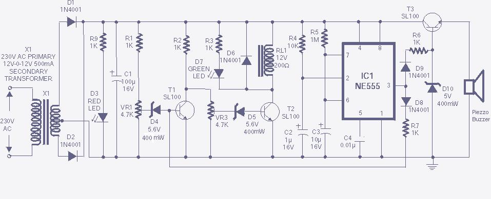
This straight forward circuit will protect electrical appliances from over voltage as well as under voltage.The circuit also produces an alarm when the power supply comes back.An ideal circuit for home to protect your valuable equipments from voltage fluctuations.The same circuit with some modifications can be used to make a automatic voltage stabilizer.

When the mains voltage is in the normal level ,the voltage at the negative terminal of zener diode D4 will be less than 5.6 Volts.At this condition transistor T1 will not conduct.The same time voltage at the negative terminal of zener diode D5 will be greater than 5.6 and so the transistor T2 will be conducting.The relay will be activated and the green LED wil be glowing.

When the mains voltage is higher than the set limit the transistor T1 becomes conducting since the voltage at the negative terminal of D4 is greater than 5.6 V.At the same time transistor T2 will be non conducting which results in the deactivation of relay to cut the mains supply from load.When the mains voltage is less than the set limit transistors T1 & T2 becomes non conducting making the relay to de- activate and cut the load from mains.Ω

The timer NE555 is wired as a monostable multivibrator with a pulse width of 10ms.When the power comes back after a cut off a negative voltage is obtained at the trigger pin which triggers the IC NE555.The transistor T3 gets forward biased and it drives the buzzer to produce a beep as an indication of power resumption.Also the transistor T1 is made on which in turn makes T2 off.As a result the relay will remain de- activate for 10ms and this provides the sufficient delay and the equipment is protected from surge voltages.

Circuit diagram with Parts list.Click to enlarge.

high-and-low-voltage-cut-of-circuit

Notes.

  • To calibrate the circuit a autotransformer is needed.Connect the output of autotransformer to the transformer primary.
  • Set the voltage to 260V and adjust VR1 to make the relay deactivated.
  • Now set the autotransformer to 160V and adjust VR2 so that the relay is de-energized.
  • VR3 can be used to vary the volume of buzzer.

Description

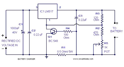
Here is a lead acid battery charger circuit using IC LM 317.The IC here provides the correct charging voltage for the battery.A battery must be charged with 1/10 its Ah value.This charging circuit is designed based on this fact.The charging curent for the battery is controlled by Q1 ,R1,R4 and R5. Potentiometer R5 can be used to set the charging current.As the battery gets charged the the current through R1 increases .This changes the conduction of Q1.Since collector of Q1 is connected to adjust pin of IC LM 317 the voltage at the output of of LM 317 increases.When battery is fully charged charger circuit reduces the charging current and this mode is called trickle charging mode.

Circuit Diagram with Parts List.

battery-charger.jpg

Notes .

  • Connect a battery to the circuit in series with a ammeter.Now adjust R5 to get the required charging current. Charging current = (1/10)*Ah value of battery.
  • Input to the IC must be minimum 15V to get 12 V for charging the battery .Take a look at the data sheet of LM 317 for better understanding.
  • Fix LM317 with a heat sink.