Description
This is the circuit diagram of a simple corrosion free water level indicator for home and industries.In fact the the level of any conductive non corrosive liquids can be measured using this circuit.The circuit is based on 5 transistor switches.Each transistor is switched on to drive the corresponding LED , when its base is supplied with current through the water through the electrode probes.

One electrode probe is (F) with 6V AC is placed at the bottom of tank.Next probes are placed step by step above the bottom probe. When water is rising the the base of each transistor gets electrical connection to 6V AC through water and the corresponding probe.Which in turn makes the transistors conduct to glow LED and indicate the level of water.The ends of probes are connected to corresponding points in the circuit as shown in circuit diagram.Insulated Aluminum wires with end insulation removed will do for the probe.Arrange the probes in order on a PVC pipe according to the depth and immerse it in the tank.AC voltage is use to prevent electrolysis at the probes.So this setup will last really long.I guarantee at least a 2 years of maintenance free operation.That’s what I got and is still going.

Components

T1 – T5 BC 548 or 2N2222 Transistors

R1-R5 2.2K 1/4 W Resistors

R6-R10 22K 1/4 W Resistors

D1 – D5 LED’s ( color your choice)

Notes

Use a transformer with 6V 500 mA output for power supply.Do not use a rectifier! we need pure AC. Use good quality insulated Aluminum wire for probes.If Aluminum wires are not available try Steel or Tin.Copper is the worst.Try the circuit first on a bread board and if not working properly, make adjustments with the resistance values .This is often needed because conductivity of water changes slightly from place to place.

Circuit Diagram and Sensor Arrangement.Click to Enlarge.

water-level.jpg

Description.

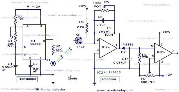
Here is the circuit diagram of an infrared motion detector that can be used to sense intrusions.Infra red rays reflected from a static object will be in one phase, and the rays reflected from a moving object will be in another phase.The circuit uses this principle to sense the motion.

The IC1 (NE 555) is wired as an astable multivibrator .The IR diode connected at the output of this IC produces infrared beams of frequency 5Khz.These beams are picked by the photo transistor Q1 .At normal condition ie; when there is no intrusion the output pin (7) of IC2 will be low.When there is an intrusion the phase of the reflected waveforms has a difference in phase and this phase difference will be picked by the IC2.Now the pin 7 of the IC 2 goes high to indicate the intrusion.An LED or a buzzer can be connected at the output of the IC to indicate the intrusion.

Circuit diagram with Parts list.

ir-motion-detector-circuit
Notes.

  • Comparators IC2a and IC2b are belonging to the same IC2 (LM1458).So the power supply is shown connected only once.No problem.
  • When there is disturbance in the air or vehicles passing nearby,the circuit may get false triggered.
  • POT R5 can be used for sensitivity adjustment.

Description.

A simple battery charger based on SCR is shown here.Here the SCR rectifies the AC mains voltage to charge the battery.When the battery connected to the charger gets discharged the battery voltage gets dropped.This inhibits the forward biasing voltage from reaching the base of the transistor Q1 through R4 and D2.This switches off the transistor.When the transistor is turned OFF,the gate of SCR (H1) gets the triggering voltage via R1 & D3.This makes the SCR to conduct and it starts to rectify the AC input voltage.The rectified voltage is given to the battery through the resistor R6(5W).This starts charging of the battery.
When the battery is completely charged the base of Q1 gets the forward bias signal through the voltage divider circuit made of R3,R4,R5 and D2.This turns the transistor ON.When the Q1 is turned ON the trigger voltage at the gate of SCR is cut off and the SCR is turned OFF.In this condition a very small amount of charge reaches the battery via R2 and D4 for trickle charging.Since the charging voltage is only half wave rectified ,this type of charger is suitable only for slow charging.For fast charging full wave rectified charging voltage is needed.

Circuit diagram with Parts list.

battery-charger-circuit-using-scr.JPG

Notes.

  • Assemble the circuit on a good quality PCB or common board.
  • The transformer T1 can be 230V primary, 18V /3A secondary step down transformer.
  • The voltage of the battery at which the charging should stop can be set by the POT R4.
  • The battery can be connected to the charger circuit by using crocodile clips.

Description.
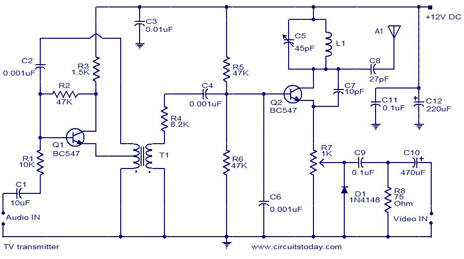
The TV transmitter given here uses UK standard 1 FM modulation for sound and PAL for video modulation. The audio signal to be modulated is pre-amplified using the transistor Q1 and associated components. The transistor Q2 has two jobs: production of carrier frequency and modulation. The pre-amplified audio signal is fed to the base of transistor Q2 for modulation. Capacitor C5 and inductor L1 forms the tank circuit which is responsible for producing the carrier frequency. The video signal is fed to the emitter of transistor Q2 via POT R7 for modulation. The modulated composite signal (audio+video) is transmitted by the antenna A1.

Circuit diagram with Parts list.

tv-transmitter-circuit

Notes.

  • Assemble the circuit on a good quality PCB.
  • Inductor L1 can be made by making 4 turns of 24SWG enameled copper wire on a 6mm dia: plastic former.
  • T1 can be a radio frequency transformer with built in capacitor. (Can be found on old transistor radio boards).
  • Antenna A1 can be a 1M long copper wire. (Experiment with the length to get optimum performance).
  • This transmitter is working in VHF band somewhat between 50 – 210MHz.
  • This transmitter is compatible only with PAL B and PAL G systems.

The above video claims you can make a pocket size FM radio station and the highlight is you dont need an antenna to do this. A small battery is enough to power and it will last for 5 to 7 hrs. This small battery powered FM radiostation even dont need a antenna to broadcast your program into the entire neighborhood for up to a mile or more . It use’s a Onboard Magnetic Loop Antenn, which is the outside copper layer. It is nothing but 2 transistors connected as a pushpull oscillator. Well, I haven’t tested this yet, so its up to you. I just thought to share this which will be useful for

Description

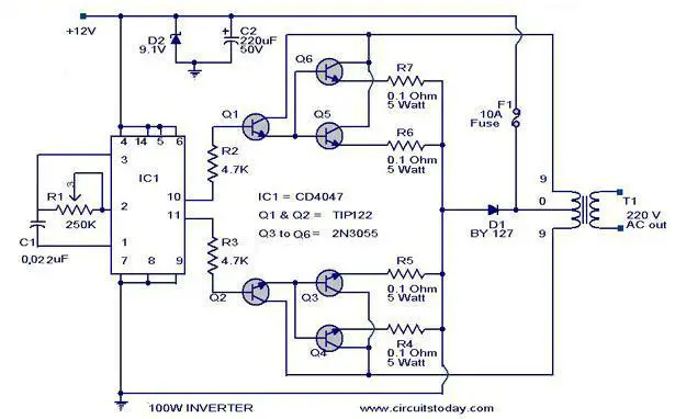
Here is a 100 Watt inverter circuit using minimum number of components.I think it is quite difficult to make a decent one like this with further less components.Here we use CD 4047 IC from Texas Instruments for generating the 100 Hz pulses and four 2N3055 transistors for driving the load.

The IC1 Cd4047 wired as an astable multivibrator produces two 180 degree out of phase 100 Hz pulse trains.These pulse trains are are preamplifes by the two TIP122 transistors.The out puts of the TIP 122 transistors are amplified by four 2N 3055 transistors (two transistors for each half cycle) to drive the inverter transformer.The 220V AC will be available at the secondary of the transformer.Nothing complex just the elementary inverter principle and the circuit works great for small loads like a few bulbs or fans.If you need just a low cost inverter in the region of 100 W,then this is the best.

Circuit Diagram with Parts List.

100-w-inverter-circuit

Notes.

  • A 12 V car battery can be used as the 12V source.
  • Use the POT R1 to set the output frequency to50Hz.
  • For the transformer get a 9-0-9 V , 10A step down transformer.But here the 9-0-9 V winding will be the primary and 220V winding will be the secondary.
  • If you could not get a 10A rated transformer , don’t worry a 5A one will be just enough. But the allowed out put power will be reduced to 60W.
  • Use a 10 A fuse in series with the battery as shown in circuit.
  • Mount the IC on an IC holder.
  • Remember,this circuit is nothing when compared to advanced PWM inverters.This is a low cost circuit meant for low scale applications.

Description.

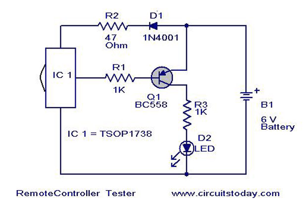
This is a simple remote controller tester circuit based on infrared sensor IC TSOP 1738. When the IR waves fall on the sensor it output changes to low state.This makes the transistor Q1 ON and LED will blink according to the code contained in the signal.So for press of each button the LED blinks in different ways.This is a good indication of the working of remote.The diode D1drops 0.7 V to give the IC ~ 5V supply from the available 6V .R2 is a current limiting resistance.

Circuit Diagram with Parts List .

remote-control-tester-circuit.jpg

Notes .

  • Use a 6V battery to power up the circuit.
  • This circuit can be used to test remotes operating in the 38Khz carrier frequency.Almost all remotes fall into this category so no problem.

Description.

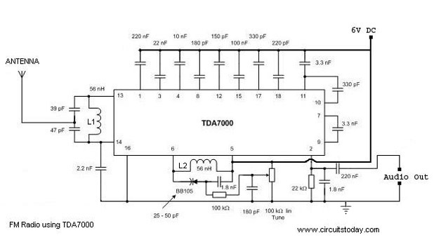
Here is a compact low cost FM radio circuit using IC7400. This circuit is designed as per the data sheet and the result is excellent.Ideal for all category of electronic enthusiasts.

The TDA7000 is a monolithic integrated circuit for mono FM portable radios, where a minimum on peripheral components is crucial. The IC TDA 7000 has a Frequency-Locked-Loop system with an intermediate frequency of 70 kHz. The intermediate frequency selectivity is achieved by active RC filters. The only function which needs alignment is the resonant circuit for the oscillator, thus selecting the reception frequency. Spurious reception is avoided by means of a mute circuit, which also eliminates too noisy input signals. Special steps are taken to meet the radiation requirements.

Circuit Diagram with Parts List. tda-7000-fm-radio-1.jpg

Notes

  • For L1 and L2 wind 5 turns of 0.6 mm enameled Copper wire on a 4 mm dia plastic former.
  • For antenna use a 50mm long insulated copper wire.
  • IC TDA 7000 can withstand up to 10 V supply voltage.But I recommend 6V.
  • Use an 8 Ohm speaker or Headphone at the audio output.

Description

Here is the circuit diagram of a simple AM transmitter circuit that can transmit your audios to your backyard.This circuit is designed with limited the power output to match the FCC regulations and still produces enough amplitude modulation of voice in the medium wave band to satisfy your personal needs.You will love this!.
The circuit has two parts , an audio amplifier and a radio frequency oscillator. The oscillator is built around Q1 (BC109) and related components. The tank circuit with inductance L1 and capacitance VC1 is tunable in the range of 500kHz to 1600KHz. These components can be easily obtained from your old medium wave radio. Q1 is provided with regenerative feedback by connecting the base and collector of Q1 to opposite ends of the tank circuit. C2 ,the 1nF capacitance , couples signals from the base to the top of L1, and C4 the 100pF capacitance ensures that the oscillation is transfered from collector, to the emitter, and through the internal base emitter resistance of the transistor Q2 (BC 109) , back to the base again. The resistor R7 has a vital part in this circuit. It ensures that the oscillation will not be shunted to ground trough the very low value internal emitter resistance, re of Q1(BC 109), and also increases the input impedance such that the modulation signal will not be shunted to ground. Q2 is wired as a common emitter RF amplifier, C5 decouples the emitter resistance and unleashes full gain of this stage. The microphone can be electret condenser microphone and the amount of AM modulation can be adjusted by the 4.7 K variable resistanceR5.

Circuit Diagram with Parts List.

am-transmitter

Notes .

  • The transmission frequency can be adjusted using the variable capacitance C3.
  • Use a 200uH inductor for the L1 in the tank circuit.
  • Power the circuit using a 9V battery for noise free operation.
  • Use a 30 cm long insulated Copper wire as the antenna.

Description

This is the schematic of a simple 40W , 12 to 220 V inverter.You don’t believe, this is simple and cheap and working for me for last 4 years.The heart of the circuit is a CD 4047 IC which is wired as an astable multi vibrator here.Resistance and Capacitance at pin 1&2 determines the out put frequency.Here it is set to 60Hz.Due to this a two 180 degree out of phase ,120 Hz , 50% dutycycle waveforms will appear at pin 10 & 11.These waves are amplified by the complementary symmetry amplifier made of transistors BC 337 & TIP 3055 to drive the out put transformer.Don’t get feared of the technical terms, just wire it on a all purpose PCB.It is simple and will work.Don’t worry about the transformer windings ,buy a 220-110-0 primary,12-0-12 secondary ,

Circuit Diagram:

Click to view in full size

simple-12-to-220-v-inverter.JPG

Tips :

First wire to oscillator part only.Then check out put Pin 10 &11 of CD4047 to obtain the required wave forms ( two 120Hz ,180 degree out of phase,50% duty cycle waves.

Description

A digital stop watch built around timer IC LM555 and 4-digit counter IC MM74C926 with multiplexed 7-segment LED display.MM74C926 consists of a 4-digit counter, an internal output latch, npn output sourcing drivers for common cathode,
7-segment display and an internal multiplexing circuitry with four multiplexing outputs.The counter advances on negative edge of the clock. The clock is generated by timer IC LM555.The circuit works off a 5V power supply. It can be easily assembled on a general-purpose PCB. Enclose the circuit in a metal box
with provisions for four 7-segment displays, rotary switch S1, start/stop switch S2 and reset switch S3
Testing

First, reset the circuit by pressing S3 so that the display shows ‘0000.’ Now open switch S2 for the stop watch to start counting the time. If you want to stop the clock, close S2. Rotary switch S1 is used to select the different time periods at the output of the astable multivibrator (IC1).

Circuit Diagram .Click to View in full size.

stopwatch-1.JPG

Description.
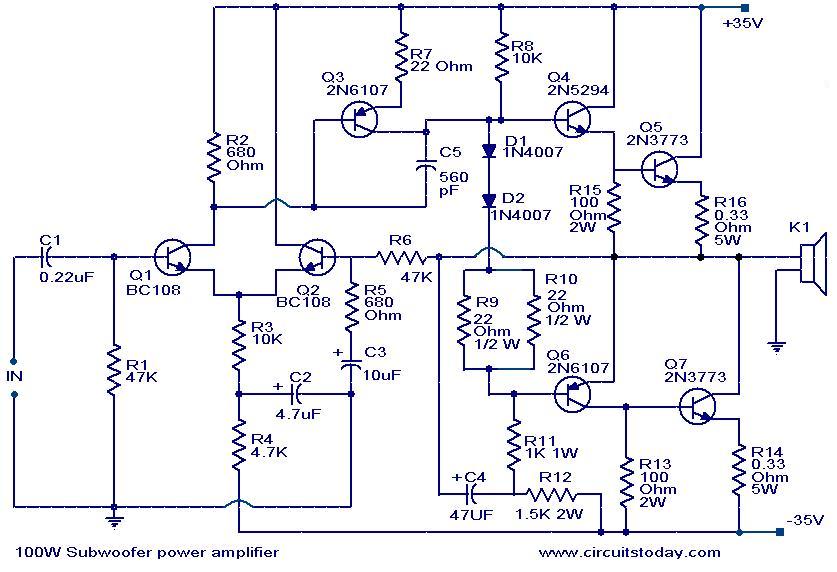
This is the circuit diagram of a fully transistorized sub woofer amplifier that can produce an output of 100W.There are seven transistors including four in the output stage. The transistors Q1 and Q2 form the preamplifier stage. Transistors Q4 to Q7 form the output stage. Since no ICs are used the circuit is very robust and can be easily assembled on a general purpose PCB.

Circuit diagram with Parts list.
100-w-subwoofer-amplifier-circuit

Notes.

  • The circuit can be powered from a +35V/-35V, 5A dual power supply.
  • Use a 100W, 12 inch sub woofer at the output.
  • All electrolytic capacitors must be rated 100V.
  • The transistor Q4 to Q7 must be fitted with heat sinks.

Description.

Here is a simple fire alarm circuit based on a LDR and lamp pair for sensing the fire.The alarm works by sensing the smoke produced during fire.The circuit produces an audible alarm when the fire breaks out with smoke.

When there is no smoke the light from the bulb will be directly falling on the LDR.The LDR resistance will be low and so the voltage across it (below .6V).The transistor will be OFF and nothing happens.When there is sufficient smoke to mask the light from falling on LDR, the LDR resistance increases and so do the voltage across it.Now the transistor will switch to ON.This gives power to the IC1 and it outputs 5V.This powers the tone generator IC UM66 (IC2) to play a music.This music will be amplified by IC3 (TDA 2002) to drive the speaker.

The diode D1 and D2 in combination drops 1.4 V to give the rated voltage (3.5V ) to UM66 .UM 66 cannot withstand more than 4V.
Circuit diagram with Parts list.

fire-alarm-circuit.JPG

Notes.

  • The speaker can be a 8Ω tweeter.
  • POT R4 can be used to adjust the sensitivity of the alarm.
  • POT R3 can be used for varying the volume of the alarm.
  • Any general purpose NPN transistor(like BC548,BC148,2N222) can be used for Q1.
  • The circuit can be powered from a 9V battery or a 9V DC power supply.
  • Instead of bulb you can use a bright LED with a 1K resistor series to it.

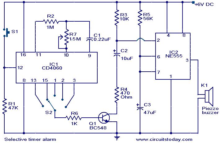
A timer circuit using IC 4060 is given here. The IC 4060 is a 14 stage binary counter with a built-in oscillator.R2, R7, C1 are the components that determine the frequency of the oscillator and the outputs will become high one after other and only one at a time. The last five outputs are only used here. The high pulses from the outputs are used to trigger the NE555 IC. Here NE555 is wired as a monostable multivibrator. The buzzer will produce the alarm when the output of IC2 goes high. The duration of the alarm depends on the components C3 and R5.The duration can be adjusted by varying the value of C3.The alarm will automatically turn OFF after the predetermined time. The trigger pin of IC2 will be normally positive. When the Q1 is forward biased by the positive pulse at its base from IC1, the capacitor C2 becomes charged and reduces the voltage at trigger pin of IC2.This triggers the IC.When the capacitor is fully charged the pin 2 becomes again positive.
The maximum duration from timer IC 4060 will be at pin 3. The times decrease by half in the pins 2, 3, 15, and 13 respectively. The timer duration can be varied by varying the capacitor C1.

Circuit diagram with Parts list.

selective-timer-alarm-circuit

Notes.

  • Use 6V DC for powering the circuit.
  • Assemble the circuit on a good quality PCB.
  • Mount the ICs on holders.
  • The switch S2 can be a single pole five throw rotary switch.
  • The switch S1 can be a push button switch.
  • S1 is used to reset the timer.
  • S2 is used to select the alarm time.
  • R7 can be used for the fine adjustment of alarm time.

  Operating Supply Voltage (VS) = 4v - 12v

The output power (POUT)
for LM386N-1, LM386M-1 at VS = 6V, RL = 8ohms, THD = 10% is 250-325 mW
for LM386N-3 at VS = 9V, RL = 8ohms, THD = 10% is 500-700 mW
for LM386N-4 at VS = 16V, RL = 32ohms, THD = 10% is 700-1000 mW.

Audio Amplifier Gain = 20 with LM386

Fig 1: LM386 Audio Amplifier with Gain = 20 and minimum part count

LM386 - Audio Amplifier with Gain=200

Fig 1: LM386 Audio Amplifier with Gain = 200

LM386 - Audio Amplifier with Bass Boost

Fig 1: Audio Amplifier with bass boost

Features

Battery operation
Minimum external parts
Wide supply voltage range: 4V-12V or 5V-18V
Low quiescent current drain: 4mA
Voltage gains from 20 to 200
Ground referenced input
Self-centering output quiescent voltage
Low distortion: 0.2% (AV = 20, VS = 6V, RL = 8Ohm, PO = 125mW, f = 1kHz)
Available in 8 pin MSOP package

Description

The LM386 is a power amplifier designed for use in low voltage consumer applications. The gain is internally set to 20 to keep external part count low, but the addition of an external resistor and capacitor between pins 1 and 8 will increase the gain to any value from 20 to 200.

The inputs are ground referenced while the output automatically biases to one-half the supply voltage. The quiescent power drain is only 24 milliwatts when operating from a 6 volt supply, making the LM386 ideal for battery operation.

Applications
AM-FM radio amplifiers
Portable tape player amplifiers
Intercoms
TV sound systems
Line drivers
Ultrasonic drivers
Small servo drivers
Power converter

he LM1875 schematic design takes advantage of advanced circuit techniques and processing to achieve extremely low distortion levels even at high output power levels. Other outstanding features include high gain, fast slew rate and a wide power bandwidth, large output voltage swing, high current capability, and a very wide supply range. The amplifier is internally compensated and stable for gains of 10 or greater.

LM1875 Features
- Up to 30 watts output power
- AVO typically 90 dB
- Low distortion: 0.015%, 1 kHz, 20 W
- Wide power bandwidth: 70 kHz
- Protection for AC and DC short circuits to ground
- Thermal protection with parole circuit
- High current capability: 4A
- Wide supply range 16V-60V
- Internal output protection diodes
- 94 dB ripple rejection
- Plastic power package TO-220

LM1875 Applications
- High performance audio systems
- Bridge amplifiers
- Stereo phonographs
- Servo amplifiers
- Instrument systems


LM1875 amplifier circuit diagram

lm1875 amplifier
LM1875 datasheet

I have been kindly submitted PCB layouts from a reader named MC Mike. He has made drawings of his own layout and mine on PCB software and has allowed me to host them here for the benefit of others.

MC's original is here, and it is provided with the following information:

.

The above is my design, the bottom is the one I followed your design from your website, choose one try resizing by printing. The parts I followed exactly from the Datasheet.
The Parts are:

R1 - 20k C1 - 1uf
R2 - 680R C2 - 220pF
R3 - 470k C3 - 3.3uF
R4 - 20k C4 - 470nF
R5 - 3.3R C5 - 22nF
R6 - 150R C6 - 220uF
R7 - 82R C7 - 470nF

Parts for your design, is exactly like your original.

.

Of many single chip hi-fi amplifiers, the TDA1514 is one of the best single chip amplifiers that you will find which is good value and good performance. It has many applications, none are suggested by the data sheet but the main application is obviously hi-fi. Here are some of my own ideas for this amplifier:

  • Stereo Hi-fi amplifier
  • Small subwoofer amplifier
  • TV amplifier (NICAM® or even mono)
  • Surround Sound Amplifier
  • PC speaker improvements, or other such speakers with built in amplifiers
  • For hi end projects this amp may also be used for mid-range or tweeter amplifiers in bi/tri amplifier systems.

First of all, lets have a description of what the TDA1514 single chip amplifier is like. Well its a single 9-pin chip that provides holes on either side for mounting onto a heatsink. It doesn't really require many more additional components and all of those are easily available. The design I used was for s split rail power supply and these are suggested as they are probably easier to build and provide a good PSU base so long as the rest of the amplifier circuitry is also split rail.

.

The circuit is a copy of the same one found in the Philips TDA1514A datasheet, found here. Writing this article, I found some shocking news that this chip is now discontinued :-( This information page is just for reference now for those who manage to get hold of the chip. I'm not sure what the new alternative is, but it better had be good Philips! :-P

As can be seen anyway, it is a little more complex then previous smaller amplifiers featured on my site, such as the TDA2040, but it is worth the extra complexity (and is still very simple anyway). Other reasons why you might want to build this amplifier are:

  • Great Value
  • High Power
  • Low distortion (harmonic and distortion)
  • Thermal Protection
  • Doesn't click when switching on and off
  • And from what I can tell, it has much better overall sound then TDA2040 chips (and the like).
  • Up to 50W of power!

If you are building this amp for lower powered applications (it will run on PSU's right down to +/-10V), then this chip will drop straight into a stripboard PCB with no awkward bending of pins and such, and other components should be accommodated with ease. I wouldn't recommend stripboard when powering this amp at over +/- 17V (from a 12V transformer) and in these cases where you do want the extra power from this amplifier, please design your own PCB with thicker tracks to handle the power better and give better sound due to lower track resistance. I designed my own board and it works very well. Even though more components are involved, the design can be almost as small as a board for the TDA2040 (and like) devices.

The ISI impact factor of the journal Nanotechnology has increased to 3.446 according to the latest ISI Journal Citation Report. The increase is especially rewarding this year as Nanotechnology has recently increased the regularity of its publications to become a weekly journal, with a resulting surge in the total number of articles published. The latest impact factor reported for the journal is indicative of the journal’s continuing prominence in a rapidly expanding community, and holds great promise for the years to come.

Intel's fledgling new desktop platform offers several new architectural advancements, in addition to native support for NVIDAI SLI technology. Though motherboard manufacturers like Asus need to have their board "certified" and enable SLI via hooks in their BIOS firmware, you can in fact now have your cake and eat it too, so to speak. Curiously, we have yet to hear from NVIDIA regarding an upcoming nForce motherboard chipset platform in support of Core i7 and from the sound of the recent banter between the two companies, we probably never will. Though, in this industry, never is a very long time. It will be interesting to see how the landscape shakes out for all parties involved.

When we think about what is perhaps the one draw-back that enthusiasts and gamers could point to with respect to an Intel chipset-based motherboard, historically, it was lack of NVIDIA SLI multi-GPU support. Though you could drop more than one AMD ATI Radeon-based graphics card into a P45, X38 or X48-chipset based motherboard, for the most part, SLI was a no-go, save perhaps for a few custom OEM solutions. This wasn't too much of a problem for gaming purists that wanted in on NVIDIA powered multi-GPU action, since there was always the most recent revision of the nForce chipset in support of Intel's platform architecture; that is of course until the launch of Intel's Core i7 platform.

The Core i7's new interconnect requires a compatible chipset, and right now, the only game in town is Intel's X58 Express. Only one component of this fresh core logic offering is actually new, though. That would be the north bridge chip, which Intel refers to as the IOH, or I/O Hub. Previous Intel chipsets have branded their north bridge components MCHs, or Memory Controller Hubs, but since the Core i7 moves the memory controller to the processor, IOH is much more fitting for the X58.

Intel manufactures the X58 IOH using 130nm process technology that feels a little antiquated given the company's fabrication prowess. After all, AMD has been building north bridge chips on a power-efficient 55nm node since March. One might expect the X58 to present a thermal challenge; however, according to at least one motherboard maker, the chip is no more difficult to cool than Intel's last flagship, the X48 Express.

Thanks to its lack of a memory controller, the X58 is a much simpler design than its predecessor. The chip is essentially a bundle of point-to-point links, the most important of which is a QuickPath Interconnect that hooks into the Core i7 processor. This interconnect is made up of a pair of 20-bit links (one for upstream and another for downstream) that push 4.8 or 6.4GT/s, depending on your choice of Core i7 processors. QPI only uses 16 bits for data (the other four are reserved for error-checking), giving the interconnect an effective 19.2 or 25.6GB/s of aggregate bandwidth—a much bigger pipe than even Intel's fastest front-side bus.


The X58 IOH

All that processor bandwidth will certainly come in handy given the fact that the X58 IOH also sports 36 lanes of second-generation PCI Express. Four of those lanes are reserved for peripherals and expansion slots, with the remaining 32 dedicated to graphics. Naturally, those graphics lanes can be split evenly between a pair of full-bandwidth x16 slots. It's also possible to arrange the lanes in a three-slot x16/x8/x8 setup and in a four-way-x8 config.

Like previous Intel chipsets, the X58 Express has full support for AMD's CrossFire multi-GPU scheme, including three- and four-way configs. SLI will also be supported—a first for Intel platforms (not including uber-expensive Skulltrail systems). However, actual SLI certification will be done at the motherboard level rather than being tied to the chipset. Certified motherboards will have a special key embedded in their BIOS that Nvidia's graphics drivers will check prior to enabling SLI. To date, Asus, DFI, ECS, EVGA, Foxconn, Gigabyte, and MSI have licensed SLI for their X58 boards. Intel is conspicuously missing from that list, though. When asked whether its X58 board would support SLI, Intel said it and Nvidia had "not found mutually acceptable business terms for certification."


The last ingredient in the X58's connectivity soup is Intel's DMI interconnect. This link offers up to 2GB/s of bandwidth, which seems a little light given the massive pipes seen elsewhere in the Core i7. However, DMI does allow the X58 to hook into Intel's existing ICH10 series south bridge chips.

Those familiar with Intel's P45 chipset will no doubt recognize the ICH10, and more specifically, the RAID-equipped ICH10R. You'd recognize this chip if you're familiar with Intel's last generation of chipsets, too, since it's little more than a die shrink of the old ICH9 series. There's nothing new here, but that's not necessarily a sign of weakness. After all, the ICH10R does pack six 300MB/s Serial ATA ports with support for novel Matrix RAID configurations and more traditional multi-drive arrays. You get a dozen USB ports, too, and an integrated Gigabit Ethernet MAC. Six gen-one PCIe lanes round out the package, offering more than enough bandwidth for onboard peripherals and expansion slots.

Overall, the ICH10R has feature parity (and in some cases, superiority) with its rivals from AMD and Nvidia. Even more importantly, the chip has proven itself to be remarkably reliable and free of niggling little issues. Given the current core logic chipset climate, that's a very good thing.

By now you've no doubt read all about Intel's new Core i7 processor. You know that the CPU otherwise known as Nehalem is based on an all-new architecture, complete with four cores (or eight, if you count Hyper-Threading), three levels of cache, an integrated memory controller, and a QuickPath Interconnect replacement for the front-side bus. You know that the Core i7 is unequivocally the fastest desktop processor around, and that in some cases, it's a fair bit quicker, clock-for-clock, than Intel's already impressive Penryn designs. Naturally, you want one. Badly.

Saddling up a Core i7 won't be as easy as plugging one of the new chips into your current system, though. Nehalem is built on a new LGA1366 package that isn't compatible with the existing LGA775 infrastructure. Without a front-side bus, the Core i7 also requires a chipset compatible with its QuickPath Interconnect: Intel's own X58 Express. You'll need a whole new motherboard to join the Core i7 party, then. But which one?

Intel has its own X58 board, of course—the latest in a series of attempts to effectively cater to overclockers and PC enthusiasts. As one might expect, Taiwanese giant Asus has an iron in the fire, too. We've had the P6T Deluxe in the labs for weeks now, and it's laden with all the rich features you'd expect from a perennial favorite.

To find out which of these two is the best option for those eager to adopt Intel's latest microarchitecture, we've run them through a grueling gauntlet of performance, peripheral, power consumption, and overclocking tests. Read on for a detailed look at the first Core i7 motherboards to make it into the Benchmarking Sweatshop.

Introducing the world’s best family of laptop processors.Δ

Now available for laptops, the Intel® Core™ i7 processor delivers unmatched technology for intelligent performance on the most demanding tasks, such as creating digital video and playing intense games.
* Overview
* Processor Numbers

Key Features

Intelligent performance when you need it
Maximize speed for demanding applications with Intel® Turbo Boost Technology◊1, which accelerates processor clock speed up to 75% to match your workload,◊2 and get better performance on highly threaded apps with the multi-threaded power of Intel® Hyper-Threading Technology◊3.

Do it all - faster
Hardcore multitaskers rejoice. The Intel® Core™ i7 processor delivers maximum processing power in response to peak demands. With the ability to multitask demanding applications faster‡1, you'll fly through everything you do on your PC - from playing intense games to creating and editing digital video, music and photos.

Amazing content creation
Unleash leading-edge digital media creation with up to 81% faster video encoding,‡2 plus incredible performance for photo editing and publishing.

Incredibly realistic gaming
Dive into a deeply immersive gaming experience with a 31% improvement in artificial intelligence for game characters and realistic physics for game worlds.‡3

Brilliantly fast

With faster, intelligent, multi-core technology that applies processing power where it's needed most, new Intel® Core™ i7 processors deliver an incredible breakthrough in PC performance. They are the best desktop processor family on the planet.¹

You'll multitask applications faster and unleash incredible digital media creation. And you'll experience maximum performance for everything you do, thanks to the combination of Intel® Turbo Boost technology² and Intel® Hyper-Threading technology (Intel® HT technology)³, which maximizes performance to match your workload.

Statistics
Manufacturer:
NVIDIA: 60% ATI: 35% Intel: 5% Other: 0%
Bus Interface:
PCI-E: 50% PCI-E 2.0: 14% PCI: 10% Other: 25%
DirectX Support:
10.0: 43% 9.0c: 23% 10.1: 15% Other: 20%
User locations:
World Map with User Locations
more statistics...
project search
Main Features

* Support NVIDIA and ATI cards
* Displays adapter, GPU and display information
* Displays overclock, default clocks and 3D clocks (if available)
* Validation of results
* No installation required
* Support for Windows 2000 / XP / Vista / Windows 7 (both 32 and 64 bit versions are supported)
* BETA SOFTWARE - please test and post feedback in the forums
* .. and yes, the author of CPU-Z has granted us permission to use a name similar to his product. Thanks Franck.

Forums

* Discussion Forum
* Test builds Forum

Screenshots

Application Screenshot Application Screenshot
Documentation

It's so simple to use, you don't need documentation.
Just download and run the binary.
Downloads

The latest version is available in the downloads section.

CPU-Z is a freeware that gathers information on some of the main devices of your system.

CPU

* Name and number.
* Core stepping and process.
* Package.
* Core voltage.
* Internal and external clocks, clock multiplier.
* Supported instructions sets.
* Cache information.

Mainboard

* Vendor, model and revision.
* BIOS model and date.
* Chipset (northbridge and southbridge) and sensor.
* Graphic interface.

Memory

* Frequency and timings.
* Module(s) specification using SPD (Serial Presence Detect) : vendor, serial number, timings table.

System

* Windows and DirectX version.

Most people don't realise this, but this is the key to your overclocking success. In order to find this, you will have to slow down your CPU, so we are completly sure your CPU isn't what's causing any problems. To do this, drop your multiplier down 2 spots from wherever it is stock. Some might argue you only need to drop your multiplier down one spot, which will more than likely work just as well, but 2 spots assures the CPU is not being pushed too far. Also, if you can set your PCI/AGP in the bios, set 33/66, respectively. With an MSI board, go ahead and set the AGP to 67 to activate the lock. Find your HTT multiplier (should have options from 2x up to 5x (socket 754 only has up to 4x max I believe)), and make sure it's at 4x. Also, disable Cool 'N Quiet if it's enabled....for some reason, it causes strange abnormalities when overclocking. Keep the FSB in the bios @ 200MHz and boot into windows.

To speed up your hard disk speed we need to configure a special buffer in the computer's
memory in order to enable it to better deal with interrupts made from the disk.

This tip is only recommended if you have 256MB RAM or higher.

Follow these steps:

Run SYSEDIT.EXE from the Run command.

Expand the system.ini file window.

Scroll down almost to the end of the file till you find a line called [386enh].

Press Enter to make one blank line, and in that line type

Irq14=4096

Note: This line IS CASE SENSITIVE!!!

Click on the File menu, then choose Save.

Close SYSEDIT and reboot your computer.

Done. Speed improvement will be noticed after the computer reboots.

Update: The most speed improvement is visible with IDE drives, however there are
reports that this tweak also does good for SCSI disks. In any case, it won't harm your
system, so why not try it yourself and let me know what you find.

Pronounced ramm, acronym for random access memory, a type of computer memory that can be accessed randomly; that is, any byte of memory can be accessed without touching the preceding bytes. RAM is the most common type of memory found in computers and other devices, such as printers.

There are two different types of RAM: DRAM (Dynamic Random Access Memory) and SRAM (Static Random Access Memory). The two types differ in the technology they use to hold data, with DRAM being the more common type. In terms of speed, SRAM is faster. DRAM needs to be refreshed thousands of times per second while SRAM does not need to be refreshed, which is what makes it faster than DRAM. DRAM supports access times of about 60 nanoseconds, SRAM can give access times as low as 10 nanoseconds. Despite SRAM being faster, it's not as commonly used as DRAM because it's so much more expensive. Both types of RAM are volatile, meaning that they lose their contents when the power is turned off.

In common usage, the term RAM is synonymous with main memory, the memory available to programs. For example, a computer with 8MB RAM has approximately 8 million bytes of memory that programs can use. In contrast, ROM (read-only memory) refers to special memory used to store programs that boot the computer and perform diagnostics. Most personal computers have a small amount of ROM (a few thousand bytes). In fact, both types of memory (ROM and RAM) allow random access. To be precise, therefore, RAM should be referred to as read/write RAM and ROM as read-only RAM.

See the "DRAM Memory Guide" in the Quick Reference section of Webopedia. This Webopedia Quick Reference offers general information on the two types of RAM and provide an overview on the common modules of each type.

A Pocket PC, abbreviated P/PC or PPC, is also known by Microsoft as a 'Windows Mobile Classic device'. It is a hardware specification for a handheld-sized computer (Personal digital assistant) that runs the Microsoft 'Windows Mobile Classic' operating system. It may have the capability to run an alternative operating system like NetBSD, Linux, Android or others. It has some of the capabilities of modern desktop PCs.

Currently there are thousands of applications for handhelds adhering to the Microsoft Pocket PC specification, many of which are freeware.[citation needed] Some of these devices also include mobile phone features. Microsoft compliant Pocket PCs can also be used with many other add-ons like GPS receivers, barcode readers, RFID readers, and cameras.

In 2007, with the advent of Windows Mobile 6, Microsoft dropped the name Pocket PC in favor of a new naming scheme. Devices without an integrated phone are called Windows Mobile Classic devices instead of Pocket PCs. Devices with an integrated phone and a touch screen are called Windows Mobile Professional devices and devices without a touch screen are called Windows Mobile Standard devices

WiMAX, meaning Worldwide Interoperability for Microwave Access, is a telecommunications technology that provides wireless transmission of data using a variety of transmission modes, from point-to-multipoint links to portable and fully mobile internet access. The technology provides up to 10 Mbit/s broadband speed without the need for cables. The technology is based on the IEEE 802.16 standard (also called Broadband Wireless Access). The name "WiMAX" was created by the WiMAX Forum, which was formed in June 2001 to promote conformity and interoperability of the standard. The forum describes WiMAX as "a standards-based technology enabling the delivery of last mile wireless broadband access as an alternative to cable and DSL".

Wi-Fi (pronounced /ˈwaɪfaɪ/) is a trademark of the Wi-Fi Alliance that may be used with certified products that belong to a class of wireless local area network (WLAN) devices based on the IEEE 802.11 standards. Because of the close relationship with its underlying standard, the term Wi-Fi is often used as a synonym for IEEE 802.11 technology.

The Wi-Fi Alliance is a global, non-profit association of companies that promotes WLAN technology and certifies products if they conform to certain standards of interoperability. Not every IEEE 802.11-compliant device is submitted for certification to the Wi-Fi Alliance, sometimes because of costs associated with the certification process and the lack of the Wi-Fi logo does not imply a device is incompatible with Wi-Fi devices.